Precision Engineering, Micro-Aperture Accuracy, and High-Yield SMT Solutions for Ireland’s Leading MedTech, Automotive, and Server Infrastructure Sectors
Get Technical ConsultationHigh-precision semiconductor and PCB assemblies optimized for the Irish electronics ecosystem, leveraging cutting-edge laser stencil technology.
Understanding the technical parameters, aperture designs, and material sciences driving zero-defect PCB assemblies.
Ireland has established itself as the premier hub for European technology, boasting a highly concentrated sector of Electronics Manufacturing Services (EMS), high-reliability MedTech devices, and Tier-1 automotive assemblies. Cities like Dublin, Galway, Cork, and Limerick are home to global giants and cutting-edge local subcontractors that require flawless solder paste deposition. The cornerstone of high-yield Surface Mount Technology (SMT) is the laser-cut SMT stencil. With the rise of sub-0201 passives, micro-BGAs, and ultra-fine-pitch QFNs, the requirements for stencil design, aperture engineering, and raw material selection have reached semiconductor-level tolerances.
In high-reliability markets, a single solder bridging or insufficient volume defect can result in catastrophic system failures—whether in an implanted medical regulator in Galway or a high-capacity cloud server array in Dublin's Silicon Docks. Thus, choosing the correct laser stencil supplier is no longer a purchasing decision; it is a critical engineering partnership. Advanced manufacturers look to partners who implement IPC-7525B Guidelines, utilize state-of-the-art fiber laser cutting heads, and offer specialized surface treatments such as fluoropolymer nano-coatings.
Deploying hydrophobic and oleophobic nano-coatings that dramatically reduce paste transfer variability, dropping bridge rates by up to 65% on ultra-fine-pitch components.
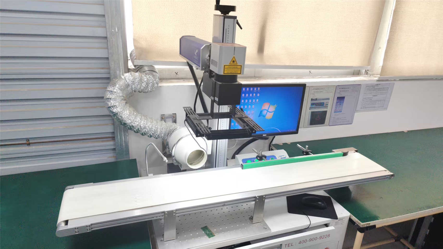
Utilizing high-power German fiber laser systems achieving cutting beam spot sizes down to 20µm with positional accuracy within ±2µm across the entire print envelope.
Strict mathematical modeling of Area Ratio (AR) and Aspect Ratio (AS) to engineer custom tapered aperture walls preventing paste retention.
A deep mathematical evaluation of area ratios required for high-yield paste release on complex assemblies.
The success of the paste printing process depends on the release coefficient. When the stencil separates from the PCB, the paste must transfer completely to the pad. Mathematically, this release is governed by the Area Ratio (AR), defined as the area of the aperture opening divided by the surface area of the aperture walls. For a rectangular aperture with length $L$, width $W$, and stencil thickness $T$:
For high-reliability medical equipment or high-frequency telecom PCBs constructed in Dublin, standard stainless steel stencils often struggle to maintain an AR below 0.66. In such instances, laser-cut fine-grain stainless steel or electroformed nickel stencils are required to lower the acceptable threshold to 0.40–0.50, especially when paired with specialized nano-coatings.
| Stencil Type | Base Material | Thickness Range | Ideal Pitch | Key Application |
|---|---|---|---|---|
| Fiber Laser Fine-Grain | FG Stainless Steel (1-2µm grains) | 80µm - 250µm | ≥ 0.4 mm pitch | Standard High-Mix Automotive, IoT, and Consumer Boards |
| Electroformed Nickel | 100% Pure Nickel Atom Lattice | 50µm - 150µm | ≥ 0.3 mm pitch | High-Density Medical Devices, CSP, Flip-Chip, and Micro-BGAs |
| Step-Up / Step-Down | Precision Etched Steel / Multi-Thickness | Multi-tiered (e.g. 100µm to 150µm) | Mixed pitch variable | RF Shielding cans combined with micro-passive layout on same board |
| Hydrophobic Nano-Stencil | FG Steel + Fluorocarbon Coating | 60µm - 200µm | ≥ 0.35 mm pitch | High-volume memory modules, telecommunication backbone routing cards |
CoreByte Storage Technology Co., Ltd. - Manufacturing Excellence, Rigorous QC, and Advanced PCB Infrastructure Since 2016
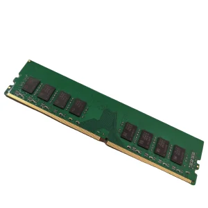
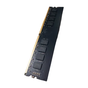
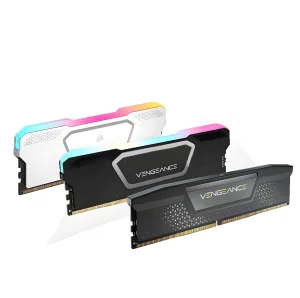
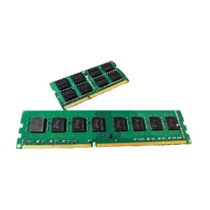
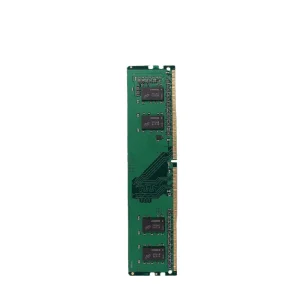
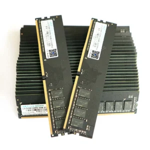
CoreByte Storage Technology Co., Ltd. is a globally recognized professional DDR5 memory, DRAM solution, and precision SMT system manufacturer. We specialize in high-performance memory modules for demanding OEM, enterprise, and cloud data center environments worldwide. Our foundational expertise in high-frequency circuit layouts, thermal dissipations, and fine-pitch PCB assemblies directly informs our high-precision manufacturing services and auxiliary SMT laser stencil support.
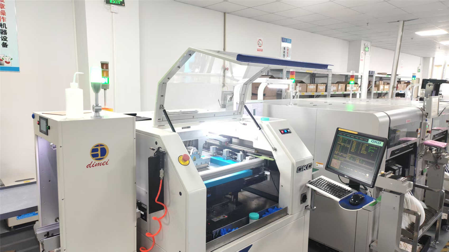
Operating a modern, highly controlled testing facility with a dedicated 320㎡ R&D Cleanroom Zone, CoreByte maintains rigorous compliance standards to service the European Union market, focusing intensively on Irish high-performance compute and high-density storage manufacturing sectors. Through a robust supply network featuring over 1,200 verified partners, we combine material sourcing, ultra-fine-pitch PCB layout design, custom stencil profiling, and thermal performance testing into a single, cohesive workflow.
Quality assurance is embedded in our DNA. We implement ISO9001-based quality management systems alongside 3D automated optical inspection (AOI), solder paste inspection (SPI), and high-temperature aging chambers to verify performance and structural stability under extreme stress conditions. For our Irish clients, this translates to reduced cycle times, complete compliance with the RoHS and REACH directives, and localized technical engineering design reviews before fabrication.


Ensuring thermal stability and structural precision in Irish industrial, computing, and communications infrastructure.
Tailoring physical configurations to meet the specific requirements of major industries across the Irish Isles.
Medical devices require extremely tight tolerances to meet Class III device requirements. Using electroformed nickel stencils ensures flat, burr-free walls that guarantee exact micro-solder volume deposition on critical pacemakers and bio-sensors.
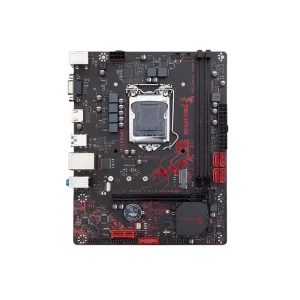
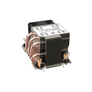
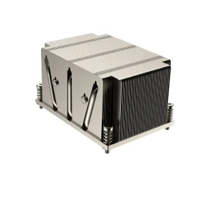
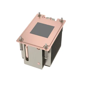
Supercomputers, artificial intelligence hubs, and high-frequency trading platforms in Dublin utilize multi-layered, copper-plated system boards. Advanced step-stencils accommodate bulky high-power connectors right next to high-density DDR5 memory pathways.
ADAS, collision avoidance systems, and electric drivetrains operate in harsh environmental conditions. The stencil design must accommodate heavy solder volumes for power components while ensuring no voiding occurs inside critical thermal pads.
How artificial intelligence and real-time process loops are changing the stencil printing landscape.
As components decrease in size, standard manual modifications of SMT apertures are giving way to automated software systems. Tomorrow’s stencil manufacturing relies on 3D Solder Paste Inspection (SPI) data loops. These systems detect insufficient or excessive paste deposition and feed that information directly back to the CAD/CAM system to automatically modify the aperture sizing for the next generation stencil build.
Furthermore, fluoropolymer nano-coatings are transitioning from a premium optional layer to an industry-standard baseline. The molecular-level coating prevents paste from sticking to the aperture walls, allowing for longer print runs with minimal dry or wet wiping. This increases line efficiency, improves output speeds, and directly lowers production costs for high-mix manufacturers operating in Western Europe.
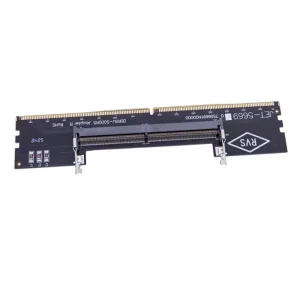
Explore our full line of memory modules, heat dissipation structures, and specialized controller cards.
Answers to complex logistical and engineering questions for production engineers and logistics departments.
Get in touch with our engineering team for specialized file optimization, SMT thickness calculations, and custom quotes designed for your assembly lines in Ireland.