Explore our top-tier high-frequency printed circuit boards, high-performance computing platforms, and server-grade hardware assemblies designed for critical applications.
Understanding transmission dynamics, dielectric losses, and substrate selection in high-speed, high-density RF system design.
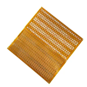
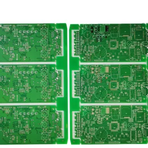
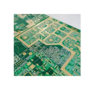
High-frequency (HF) printed circuit boards represent the physical backbone of the modern telecommunication, radar, and aerospace industries. As operating frequencies expand from standard gigahertz (GHz) bands towards millimeter-wave (mmWave) regions, standard FR-4 substrates encounter significant physical bottlenecks. Factors like dispersion, conductor loss, dielectric breakdown, and impedance mismatches can critically degrade high-speed signal integrity. Selecting appropriate high-frequency laminates, such as Rogers 4000 series (RO4003C, RO4350B) or specialized Shengyi High-TG (TG170) FR-4, is key to managing propagation delay and minimizing insertion loss.
Designing multi-layer high-frequency assemblies often involves a hybrid mixed-pressure stackup. To balance material budgets with signal integrity, engineers pair expensive PTFE or hydrocarbon laminates (e.g., Rogers 4000) on critical outer RF microstrip layers with cost-effective, high-reliability structural materials like Shengyi High-TG FR-4 for inner routing and power distribution. Achieving clean hybrid stackups requires precise lamination parameters, specialized resin chemistry matching, and precise registration control during high-temperature pressing cycles.
Deploying high-frequency engineering solutions from 5G telecom architectures to edge intelligence and high-density compute nodes.
Deploying massive MIMO antennas, remote radio heads, and Base Transceiver Stations (BTS) requires microstrip transmission lines with strict impedance tolerances. Our low-loss hybrid PCBs minimize signal distortion in sub-6GHz and mmWave deployments, ensuring high data throughput with low power consumption.
Next-generation automotive safety depends on 77GHz and 81GHz radar transceivers. Operating at these wavelengths demands highly stable substrate thickness and low conductor surface roughness (typically using VLP copper foils) to prevent phase skew, supporting high-speed collision avoidance systems.
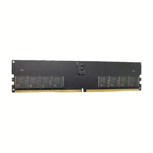
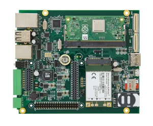
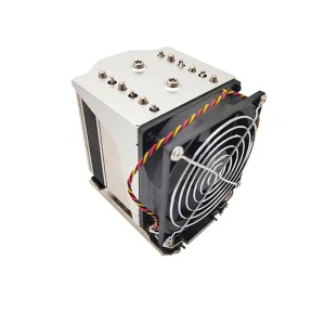
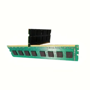
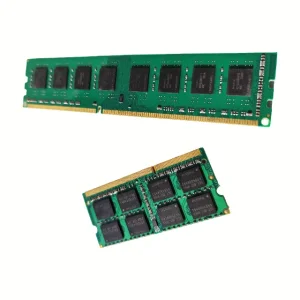
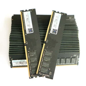
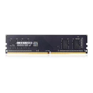
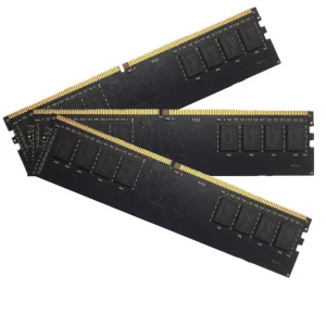
Modern data centers utilize accelerators with NPUs, high-performance DRAM (like DDR4/DDR5), and server processors. Processing billions of parameters at gigahertz rates demands precise impedance alignment, clean ground planes, and low-loss substrates to maintain signal integrity in dense multi-layer computing environments.
Analyzing the global supply chain dynamics, regional manufacturing capabilities, and industrial demand for RF laminates.
The global market for high-frequency PCBs is growing rapidly, driven by the rollout of 5G infrastructure, satellite communication networks, and artificial intelligence hardware. Currently, manufacturing is centered in East Asia, particularly in mainland China and Taiwan, with expanding sourcing hubs across Southeast Asia. High-frequency copper clad laminates (CCL) rely on specialized material suppliers, requiring close cooperation between component manufacturers and raw material providers to secure a stable supply chain.
System integrators and global buyers face ongoing challenges around material availability, price fluctuations, and strict environmental compliance. Standardizing stackup configurations (using readily available substrates like Rogers RO4350B and RO4003C alongside equivalent high-TG FR-4 from brands like Shengyi) helps mitigate supply chain risks. Optimizing trace layouts and stackup designs reduces the layer count of expensive materials, allowing developers to maintain performance targets while managing production costs.
Enterprise-grade memory modules, customized hardware designs, and integrated semiconductor solutions.
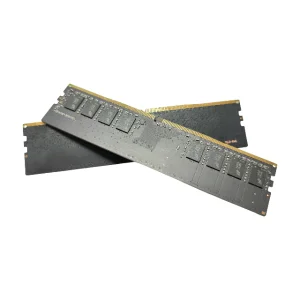
CoreByte Storage Technology Co., Ltd. is a professional DDR5 memory and DRAM solution manufacturer specializing in high-performance memory modules for global OEM, enterprise, and data center applications. Established in 2016, the company has developed strong capabilities in R&D, production, and international trade, focusing on stable, high-speed, and energy-efficient memory products.
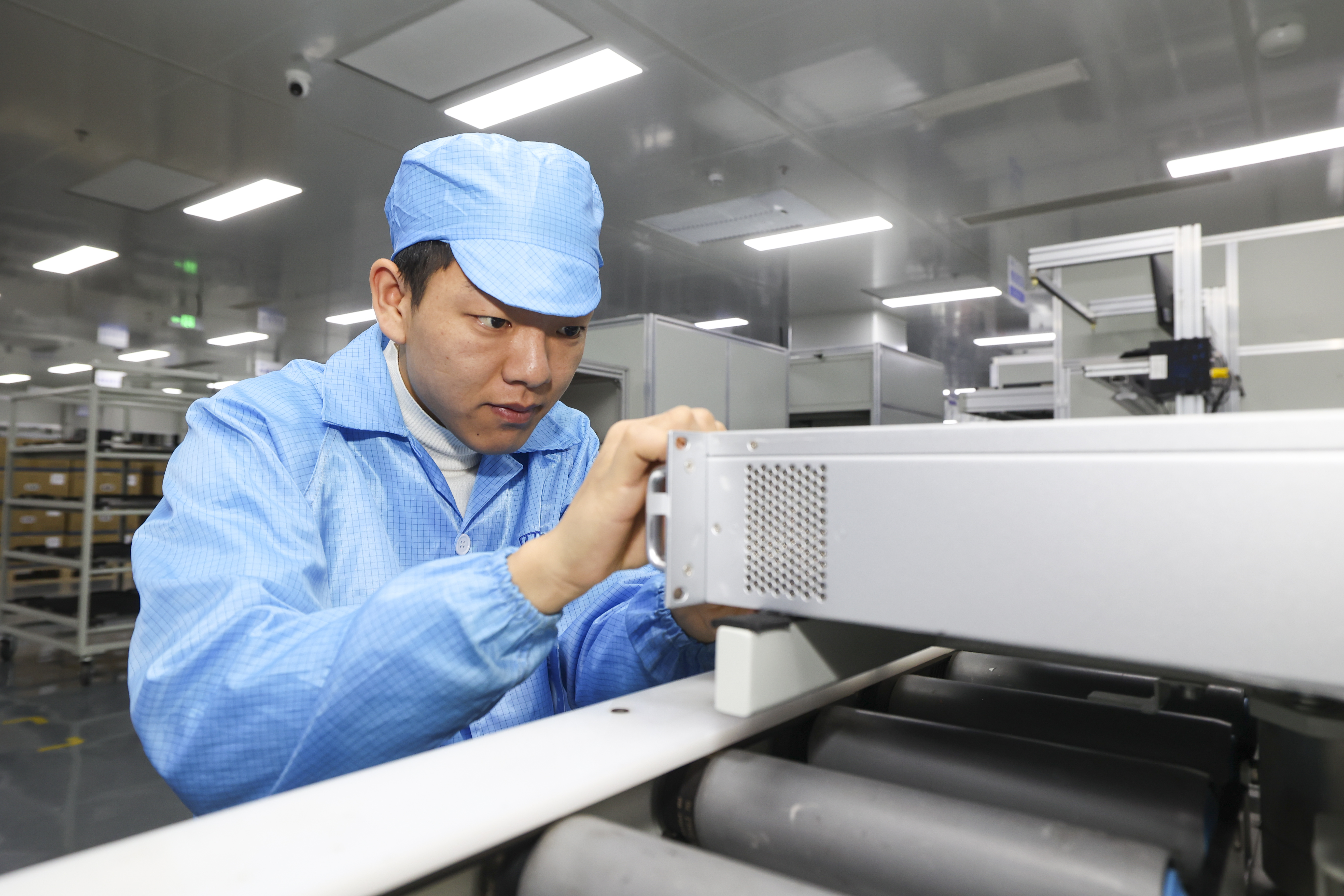
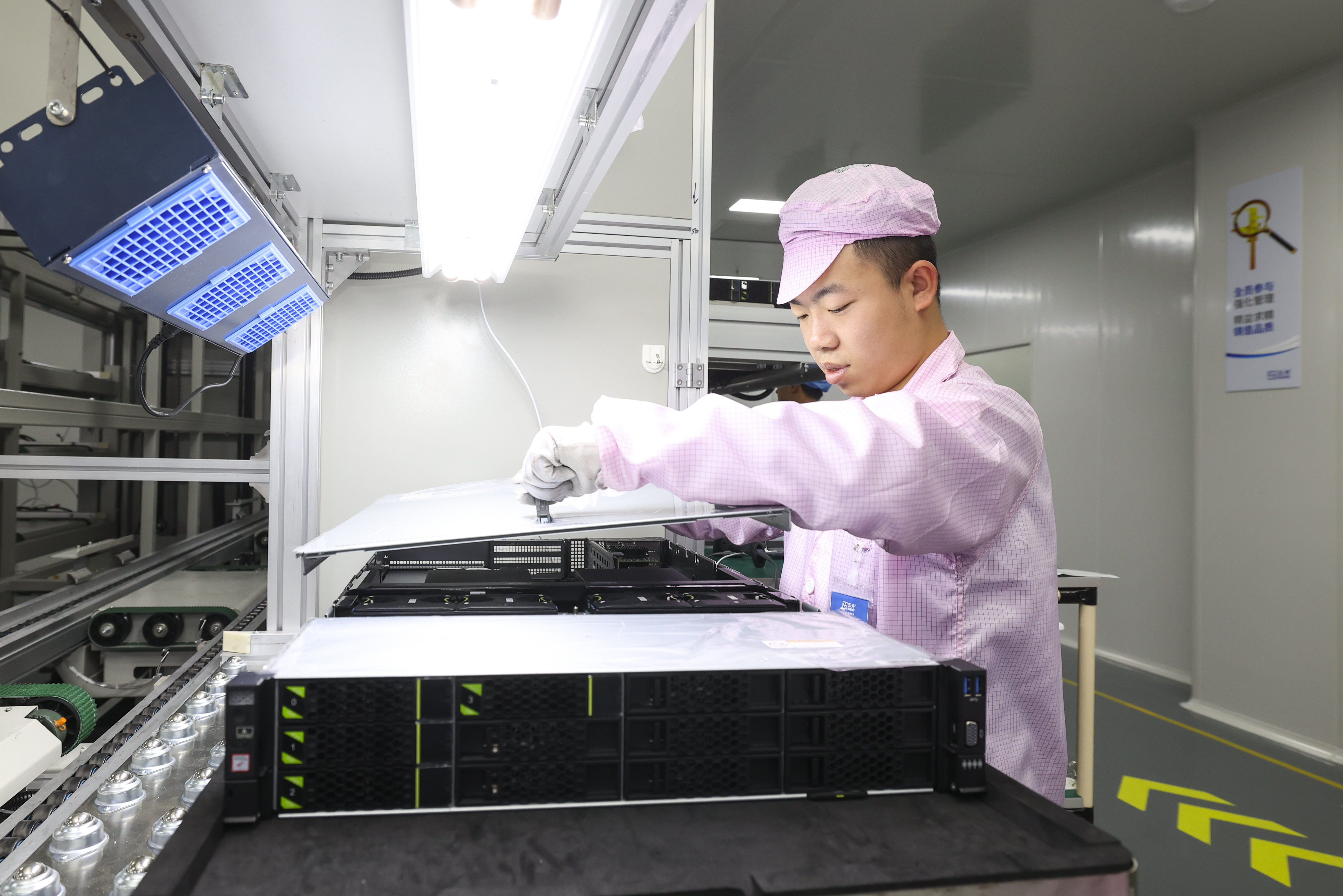
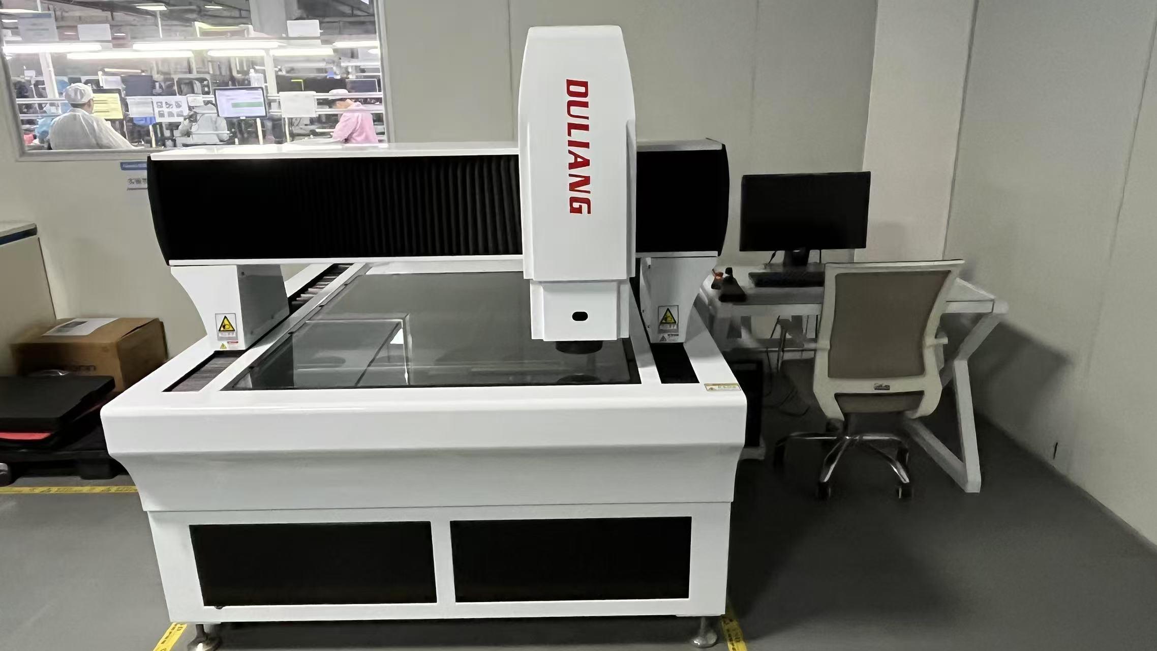
The company operates a modern manufacturing facility with a total building area of approximately 320㎡, equipped with advanced production and testing equipment to ensure strict quality control standards. CoreByte has an annual export revenue of around USD 12 million, with 6 years of export experience and over 9 years of industry experience in memory and semiconductor-related solutions.
Quality assurance is a core priority at CoreByte. The company implements ISO9001-based quality management systems, combined with automated optical inspection (AOI) and high-temperature aging tests to ensure product stability and compatibility. The quality control team consists of 45 dedicated inspectors, ensuring every batch meets international performance standards.
CoreByte maintains a strong trade-oriented business background, serving key markets including North America, Europe, Southeast Asia, and the Middle East. The company has established a reliable global supply chain network with more than 1,200 supply chain partners, supporting stable production and fast delivery.
Its primary customers include OEM system integrators, server manufacturers, industrial computer brands, and data center solution providers. With strong engineering capabilities, CoreByte offers advanced customization services, including PCB design optimization, frequency tuning, thermal solution adjustment, and branding customization.
The company invests heavily in innovation, with 85 R&D engineers and launching approximately 120 new product models annually to meet evolving market demands in AI computing, cloud infrastructure, and high-performance gaming systems.
Adhering to strict international quality standards, lead-free processing, and global environmental mandates.
Operating as a reliable high-frequency PCB supplier and memory exporter requires compliance with strict international regulatory frameworks. To support our clients globally, we enforce comprehensive RoHS (Restriction of Hazardous Substances) and REACH compliance, utilizing eco-friendly, lead-free surface finishes such as lead-free HASL, ENIG (Electroless Nickel Immersion Gold), and ENEPIG. These finishes protect copper traces from oxidation and guarantee high solder joint reliability across repeated thermal cycles.
Our manufacturing and assembly sites operate under strict quality management frameworks, aligning with the following standards:
Through our established global distribution network, we offer localization support to key markets in Europe, North America, Southeast Asia, and the Middle East. Our logistics processes are structured to support duty-unpaid or customs-cleared shipments directly to manufacturing lines, minimizing lead times and simplifying supply chain management.
Anticipating the requirements for sub-terahertz communications, ultra-low loss copper foils, and next-generation packaging.
As industry standards transition from 5G to 6G and cloud computing requirements expand, high-frequency design requirements are shifting. Future applications operating in sub-terahertz bands require substrate materials with exceptionally low dielectric loss. We are tracking these requirements by evaluating ultra-low loss materials like Liquid Crystal Polymer (LCP) and Modified Polyimide (MPI), which offer high dimensional stability and low water absorption for flexible and high-speed applications.
Conductor loss becomes a primary attenuation source at extremely high frequencies. To address this, we are integrating ultra-thin, low-profile copper foils, such as Very Low Profile (VLP) and Hyper Very Low Profile (HVLP) copper, to mitigate skin effect losses at frequencies above 28 GHz. Standardizing these technologies helps ensure that next-generation high-frequency PCBs and high-speed memory systems can support the data rates required by modern AI networks and advanced industrial hardware.
Answers to common engineering queries regarding high-frequency PCB fabrication, stackups, and memory module integration.
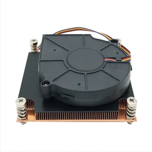
Review our custom multilayer PCB manufacturing capabilities, flexible circuit lines, server-grade DDR memory, and cooling solutions.