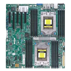
Los Angeles has evolved from a historic aerospace manufacturing cluster into a global epicenter for complex power electronics, commercial space exploration, and sustainable energy technology. Centered around major aerospace hubs in El Segundo, Long Beach, and Pasadena, alongside Silicon Beach's tech corridors, the Southern California market imposes unique operating parameters. Today’s industrial applications reject generic circuit design; they require extreme reliability under extreme conditions. This demands the deployment of Thick Copper PCBs (ranging from 3 oz to upwards of 20 oz of copper thickness).
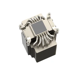
In aerospace applications, particularly for low Earth orbit (LEO) satellites and launch vehicle telemetry, electronics must function in near-vacuum states where convective air cooling is nonexistent. Heat dissipation must occur through conduction. Thick copper layers act as integrated heat sinks, pulling heat directly from power MOSFETs and microprocessors and routing it toward the external structural frame. Local electric vehicle (EV) developers and fast-charging network integrators throughout Southern California require heavy copper boards to handle high current loads of up to 400A without exceeding critical glass transition temperatures ($T_g$).
Furthermore, localized power grid distribution systems and industrial automation networks in Los Angeles rely on heavy copper layers to mitigate the risk of catastrophic failures. By choosing localized design collaboration paired with structured global manufacturing pipelines, Los Angeles procurement groups achieve optimized cycles that balance rapid prototyping compliance with mass-scale cost controls.
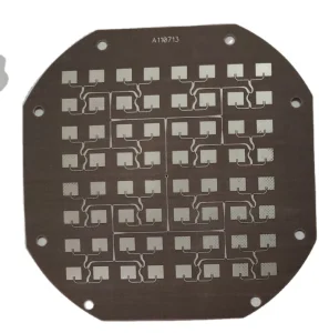
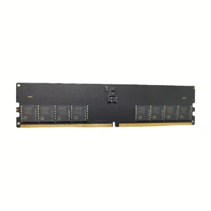
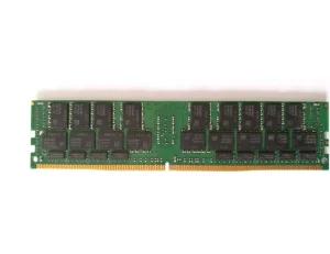
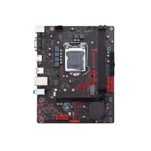
Engineering a thick copper PCB requires an understanding of advanced electrochemistry, material properties, and thermal dissipation metrics. Standard PCBs typically leverage 1 oz ($35\mu m$) or 2 oz ($70\mu m$) copper weights. In contrast, heavy copper designs occupy the range of 3 oz to 10 oz ($105\mu m$ to $350\mu m$), while extreme copper configurations can exceed 20 oz ($700\mu m$).
The core challenge of thick copper fabrication is avoiding "undercutting" during the chemical etching phase. As the copper thickness increases, lateral etching can degrade trace geometry. CoreByte uses advanced differential etching systems to maintain vertical sidewall profiles, preserving precise impedance values.
Standard FR4 substrates exhibit low thermal conductivity ($~0.25 \text{ W/m}\cdot\text{K}$). By integrating internal thick copper planes ($385 \text{ W/m}\cdot\text{K}$) and thermal vias, thermal energy is distributed across the entire structure, dropping junction temperatures by up to $35^{\circ}\text{C}$.
Mismatches in the Coefficient of Thermal Expansion (CTE) between the heavy copper structures and dielectric materials (such as high-Tg FR4, Taconic, or Rogers) can lead to delamination under cycling. Precise curing parameters and resin selection eliminate internal stress points.
By implementing these methodologies, designers in aerospace and industrial sectors can minimize their assembly volumes, replacing mechanical busbars with direct, on-board traces that manage power distribution safely and compactly.
CoreByte Storage Technology Co., Ltd. is an industry-leading DDR5 memory, DRAM solution, and complex multi-layered circuit board assembly manufacturer. We serve system integrators, aerospace subcontractors, and global data centers with robust component designs engineered to perform under heavy workloads. Established in 2016, we combine semiconductor expertise with printed circuit board co-design, offering thermal management solutions to clients worldwide.
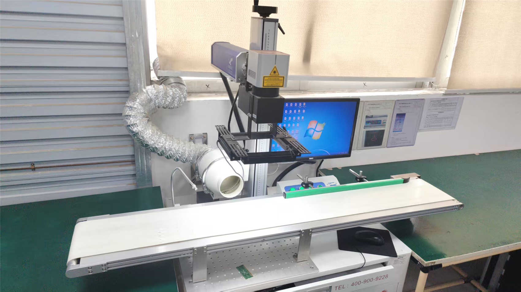
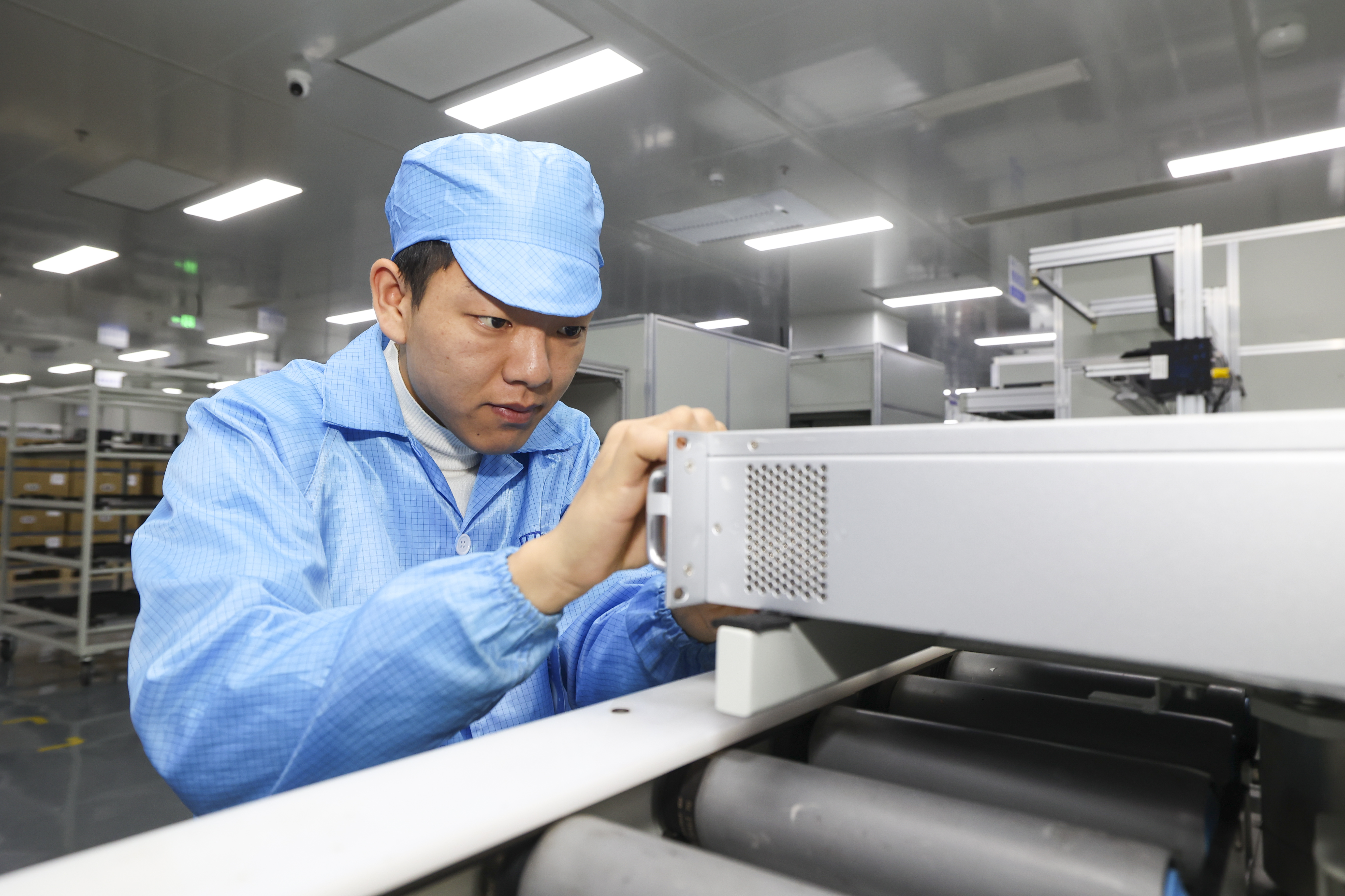
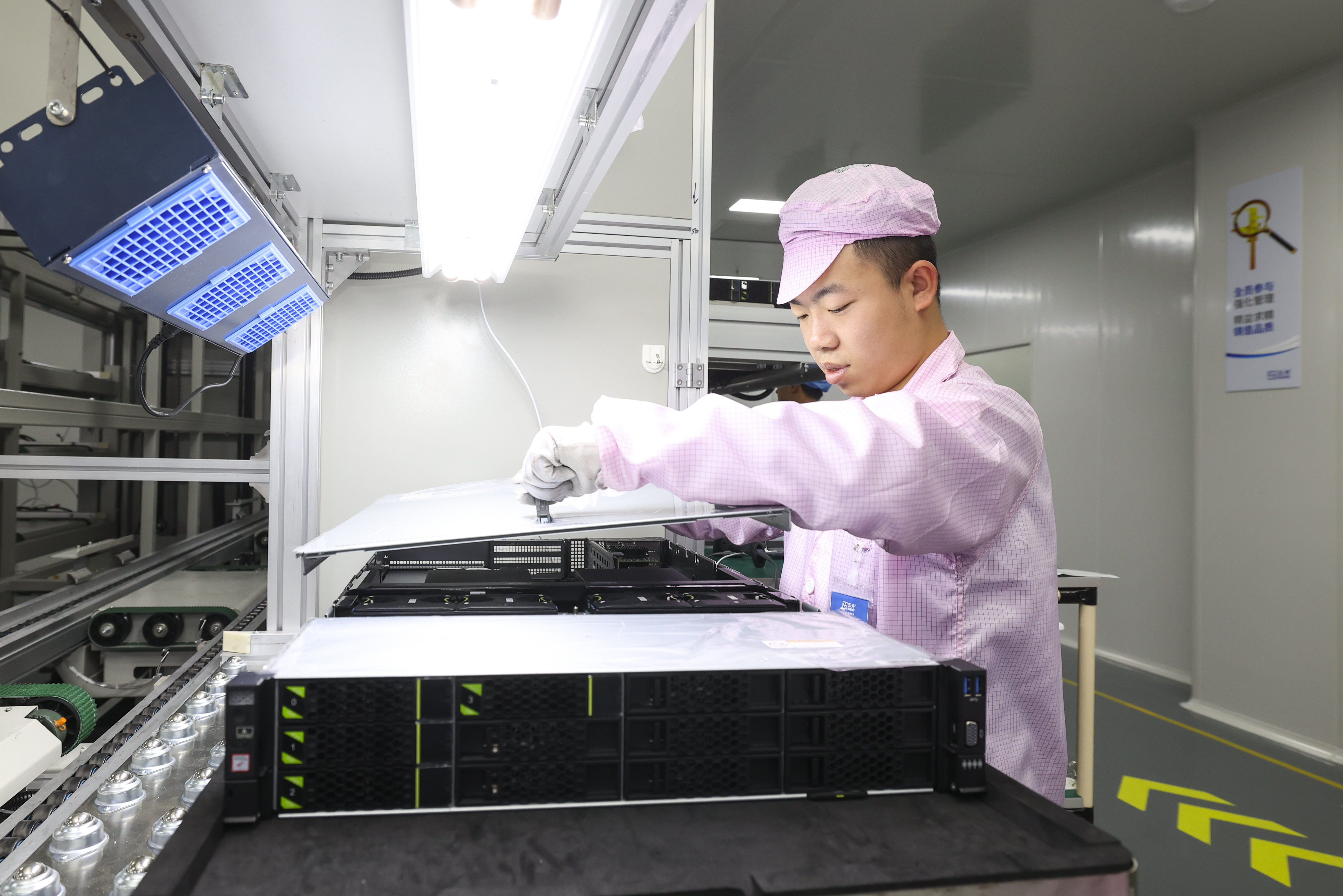
Operating a manufacturing footprint optimized for quick-turn validation and rigorous quality screening, CoreByte implements robust ISO9001-based quality management systems. Every assembly undergoes automated optical inspection (AOI), high-temperature aging tests, and multi-layer impedance sweeps. With over 9 years of domain experience, CoreByte supports custom PCB engineering, frequency optimization, and thermal layout configurations, delivering up to 120 new product models annually.
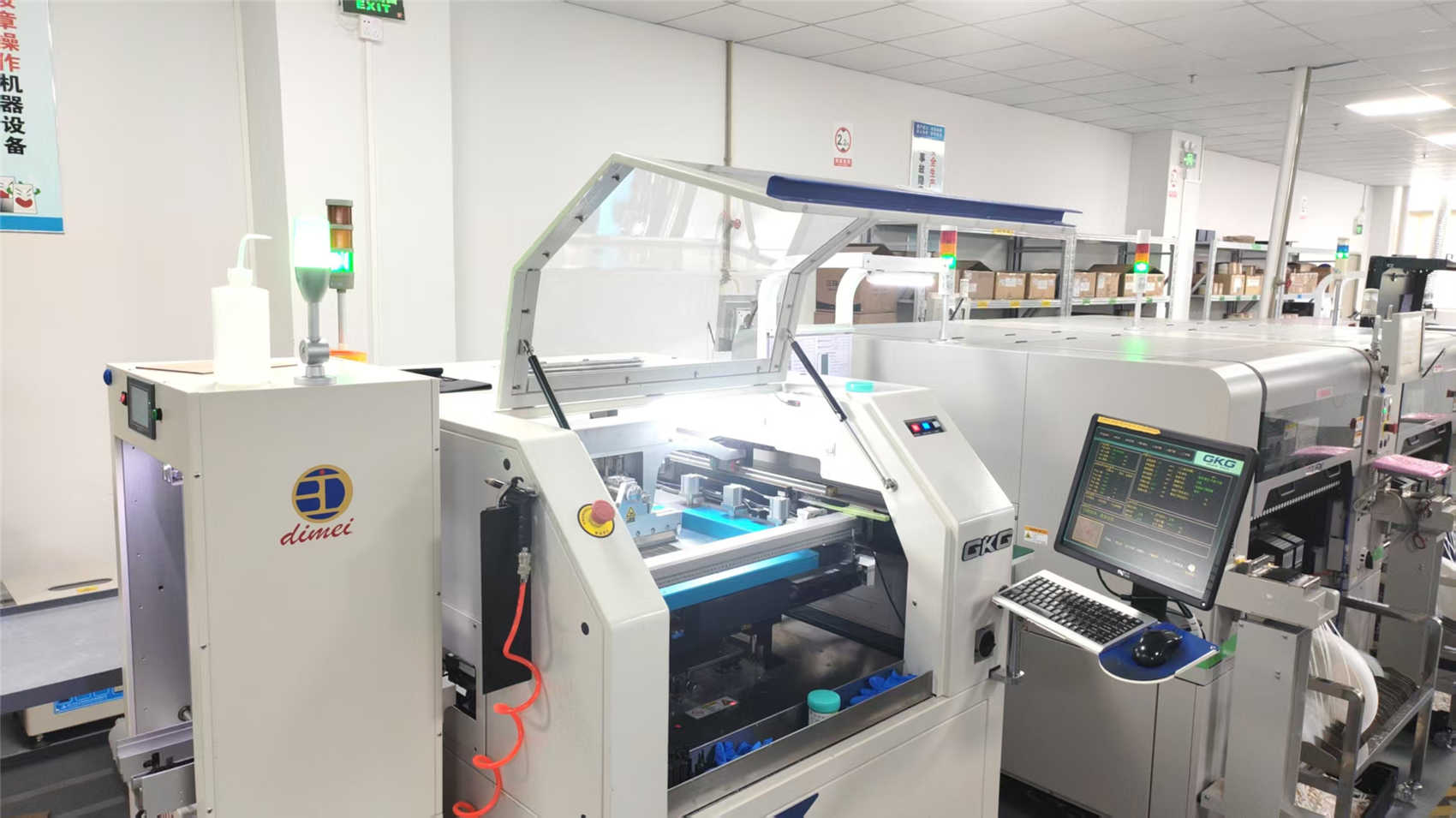
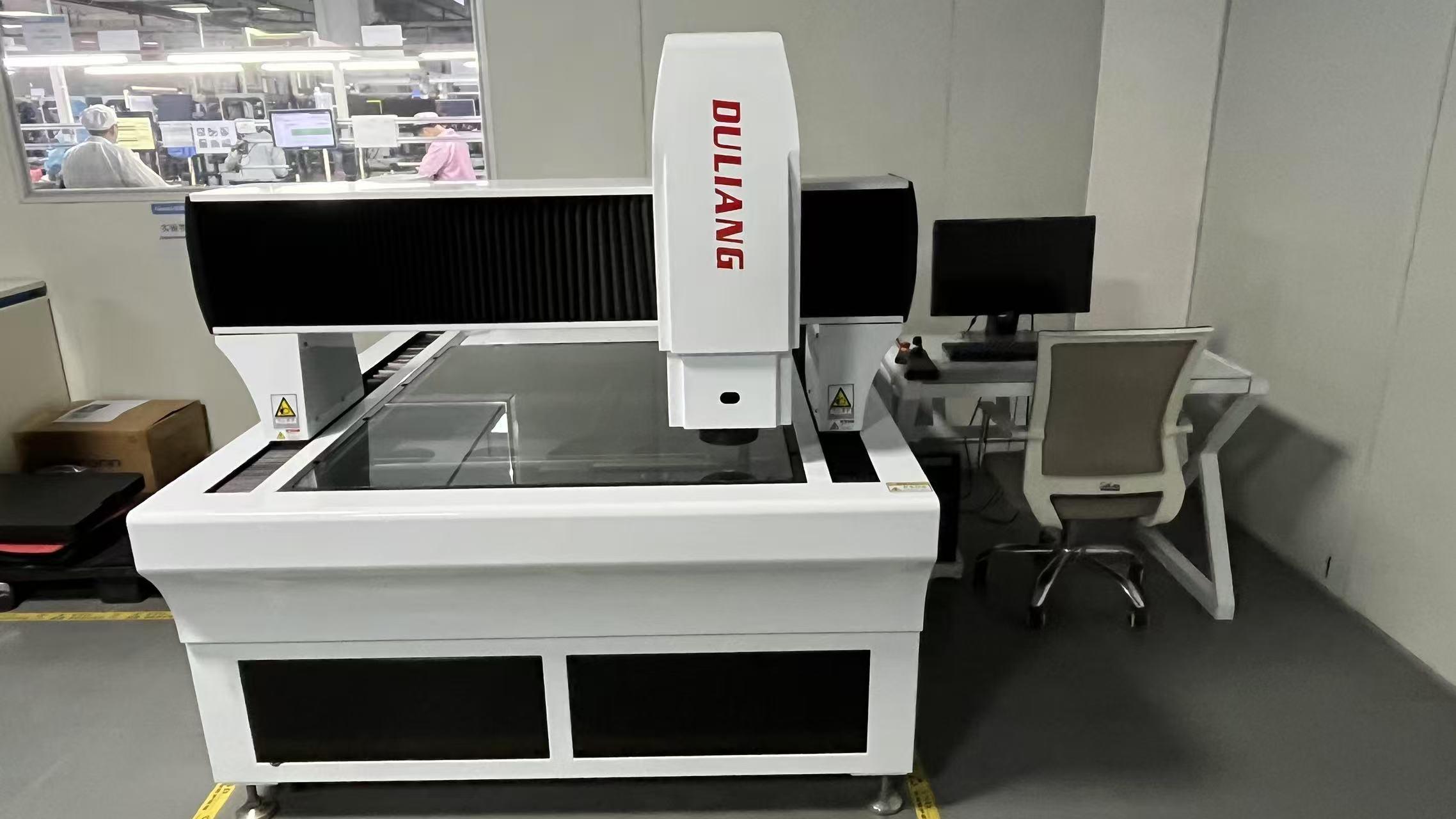
Sourcing high-reliability electronics involves balancing cost, lead times, and engineering rigor. By utilizing China’s advanced Industry 4.0 manufacturing ecosystems, Los Angeles buyers can bridge the gap between local prototyping agility and cost-efficient mass production. Industry 4.0 facilities leverage smart automation, real-time raw material tracking, and optical inspection arrays that monitor trace deposition at the micron level.
This automated framework minimizes the variability common in high-mix, low-volume productions. For thick copper boards, where chemical concentration deviations, temperature shifts, or plating speeds can affect trace profiles, automated closed-loop control systems ensure uniform copper distribution across large panels. This level of quality control reduces the risk of field failures in critical industrial systems.
CoreByte offers a structured dual-source model: engineers in Southern California manage the initial schematic validation and mechanical design files (DFM checks), while CoreByte’s manufacturing facility in China handles production scaling, advanced component sourcing, and rigorous thermal cycle testing. This model helps mitigate supply chain risks and reduces overall time-to-market.
In high-power industrial and defense applications, regulatory compliance is non-negotiable. Products must conform to strict performance and safety standards, particularly when operating within aerospace and defense sectors. Our manufacturing and sourcing pipelines align with the following regulatory frameworks:
IPC-6012 Class 3 / 3A: Heavy copper fabrication requires adherence to IPC-6012 standards, specifying structural requirements for rigid printed boards. Class 3 covers high-reliability electronic products where continued performance or performance-on-demand is critical, and equipment downtime cannot be tolerated, such as in aerospace life-support systems or military hardware.
UL 94V-0 Flammability Rating: Due to the potential thermal risks of high-current paths, all dielectric materials and substrates utilized in our heavy copper boards carry UL 94V-0 ratings, ensuring rapid self-extinguishing characteristics in the event of an electrical fault. Furthermore, RoHS compliance is strictly maintained across our production lines, minimizing toxic substances in electronic waste.
Get in touch with our Los Angeles procurement partners and global engineering team to request custom PCB design review, thermal engineering feedback, or dynamic component supply options.
Send Inquiry Now