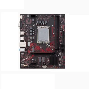
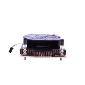
High-reliability hardware modules, optimized thermal components, and heavy-duty circuit architectures engineered for modern industrial deployments.
Exploring the macroeconomic drivers, industrial transformations, and specific design mandates forcing the transition to thick copper PCBs in the heart of Europe.
Luxembourg, recognized as one of Europe's premier industrial innovation and logistics corridors, has rapidly transitioned its economic focus toward advanced electronics manufacturing, clean technologies, automotive intelligence, and aerospace engineering. As the country aligns with the European Union’s strict climate neutrality deadlines and coordinates its national digital-first strategy, local companies are experiencing an unprecedented surge in demand for power electronic modules. The shift from low-voltage microelectronics to high-capacity power distribution platforms has placed Thick Copper PCBs (Heavy Copper PCBs) at the core of new engineering architectures.
Industries across Esch-sur-Alzette, Clervaux, and Luxembourg City’s high-tech parks require robust circuits capable of carrying substantial electrical current while handling intensive thermal energy dissipation. The integration of electric vehicle (EV) charging stations, renewable grid infrastructure, solar power storage, and custom satellite telecommunications systems has made standard PCBs obsolete for heavy industrial applications. High-power density demands can only be addressed by thicker copper layers that provide a lower thermal resistance path, protecting sensitive digital components from thermal fatigue.
Understanding copper weight limits, structural stackups, and thermal management metrics required for robust European standards.
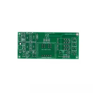
For an electronic engineer, selecting the correct copper thickness is not merely a pricing choice; it determines the system's operational ceiling. Standard printed circuit boards utilize a copper thickness of 1 oz/ft² (35 µm). In contrast, Thick Copper PCBs feature copper weights ranging from 3 oz/ft² (105 µm) to over 20 oz/ft² (700 µm). This thick-metallization profile ensures a substantial reduction in I²R conduction losses and effectively dissipates concentrated thermal loads.
| Copper Weight (oz/ft²) | Copper Thickness (µm) | Current Carrying Capacity (Amp, Trace Width: 10mm) | Primary Industrial Use-Case | Dielectric Material Recommendation |
|---|---|---|---|---|
| 3 oz | 105 µm | ~45 A | Data center server power supplies, high-current relays | FR4 TG170 / TG180 |
| 4 oz - 6 oz | 140 µm - 210 µm | ~65 A - 95 A | EV charging systems, onboard chargers (OBC), motor controllers | High TG Epoxy FR4, Polyimide |
| 8 oz - 12 oz | 280 µm - 420 µm | ~120 A - 170 A | Smart grid distribution units, solar central inverters, railway systems | High TG Ceramic Filled FR4 |
| 15 oz+ (Heavy Copper) | 525 µm+ | >200 A | Heavy military machinery power distribution, severe environment switches | Metal Clad Base / Specialized IMS |
Etching thick copper layers requires highly specialized chemical controls to prevent over-etching, trace undercutting, and non-uniform surface distribution. As the copper thickness climbs, standard lithographic processes fail, and suppliers must rely on advanced multi-pass dry film laminations and optimized acidic spray systems. Additionally, applying the liquid photoimageable (LPI) solder mask over high-profile copper tracks requires custom screen-printing matrices and multiple coatings to ensure there are no air bubbles trapped adjacent to the trace sidewalls.
Combining deep semiconductor expertise with robust PCB thermal engineering solutions for Luxembourg and the broader European market.
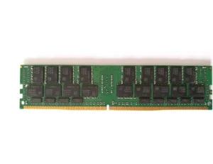
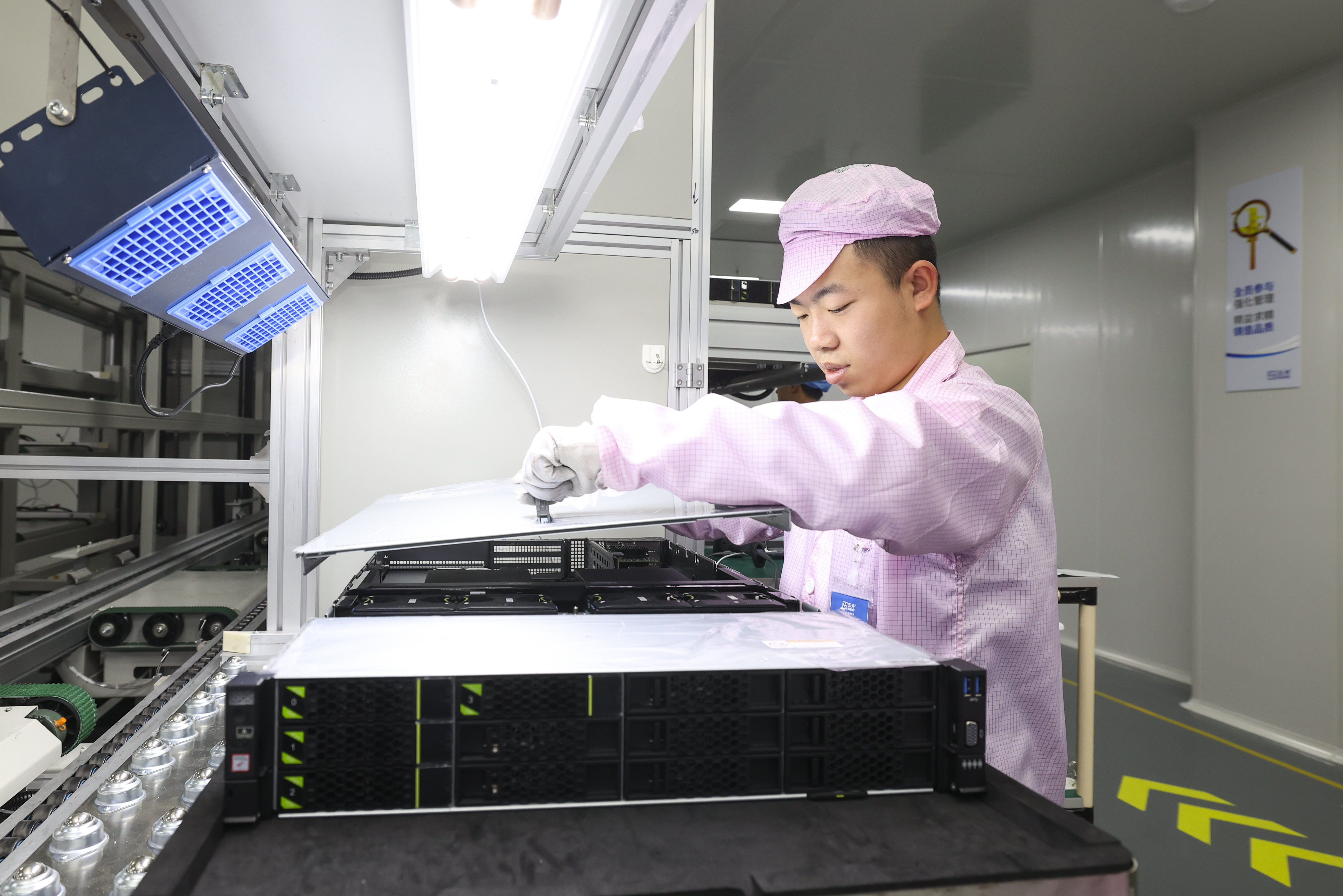
CoreByte Storage Technology Co., Ltd. is a leading DDR5 memory, DRAM solution, and advanced thermal-management PCB manufacturer specializing in high-performance computing, enterprise storage, and high-reliability industrial circuit assemblies. Founded in 2016, the company has integrated years of semiconductor production knowledge with advanced substrate manufacturing to deliver world-class high-current PCB solutions for OEM, enterprise, and smart-grid applications worldwide.
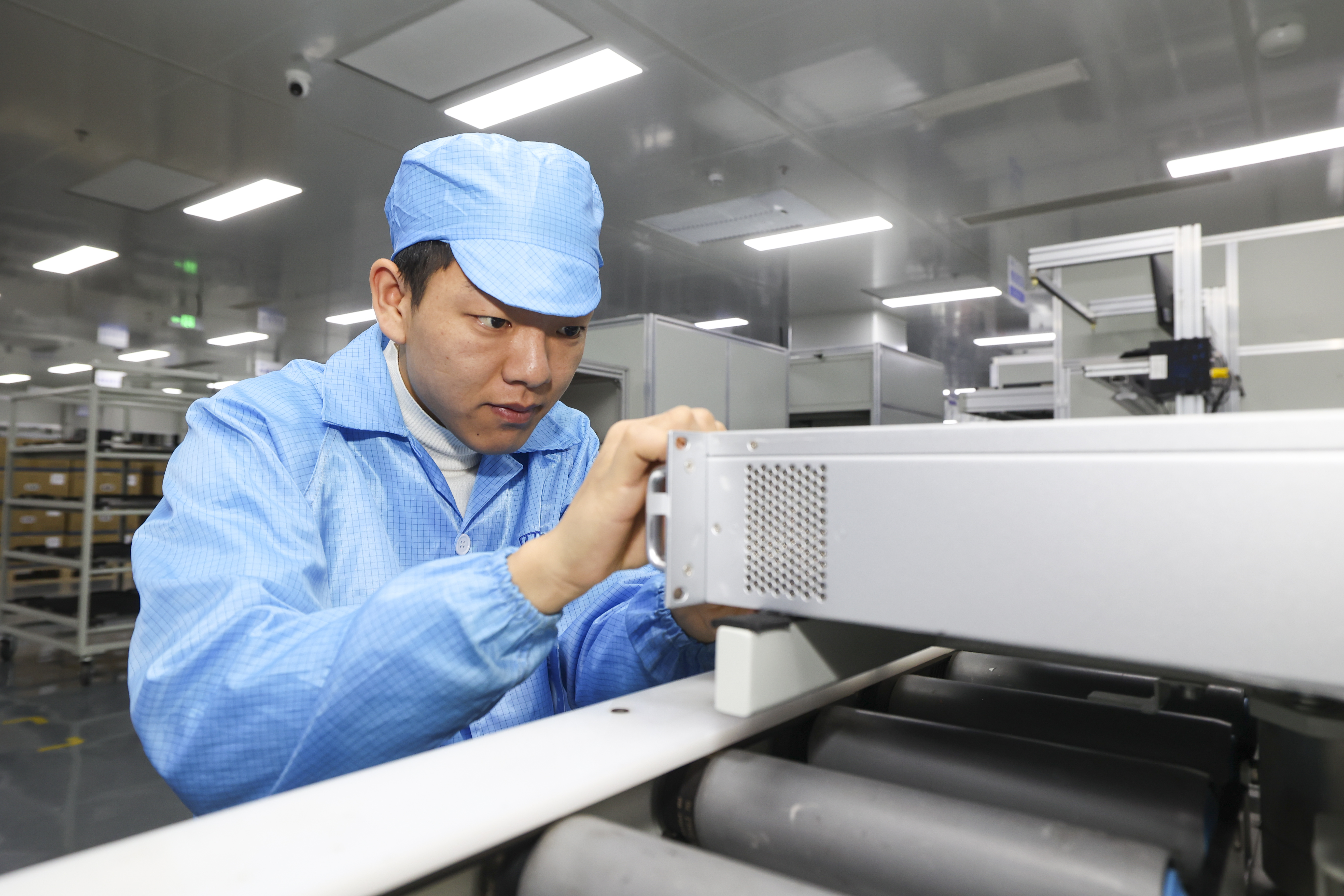
Operating a modernized, highly automated manufacturing footprint spanning 320㎡ of cleanroom environments and testing labs, CoreByte enforces rigorous quality protocols. Backed by 6 years of global export experience and over 9 years of hardware industry innovation, we serve top-tier OEM system integrators, server manufacturers, and industrial automation firms in North America, Europe, and the Middle East.
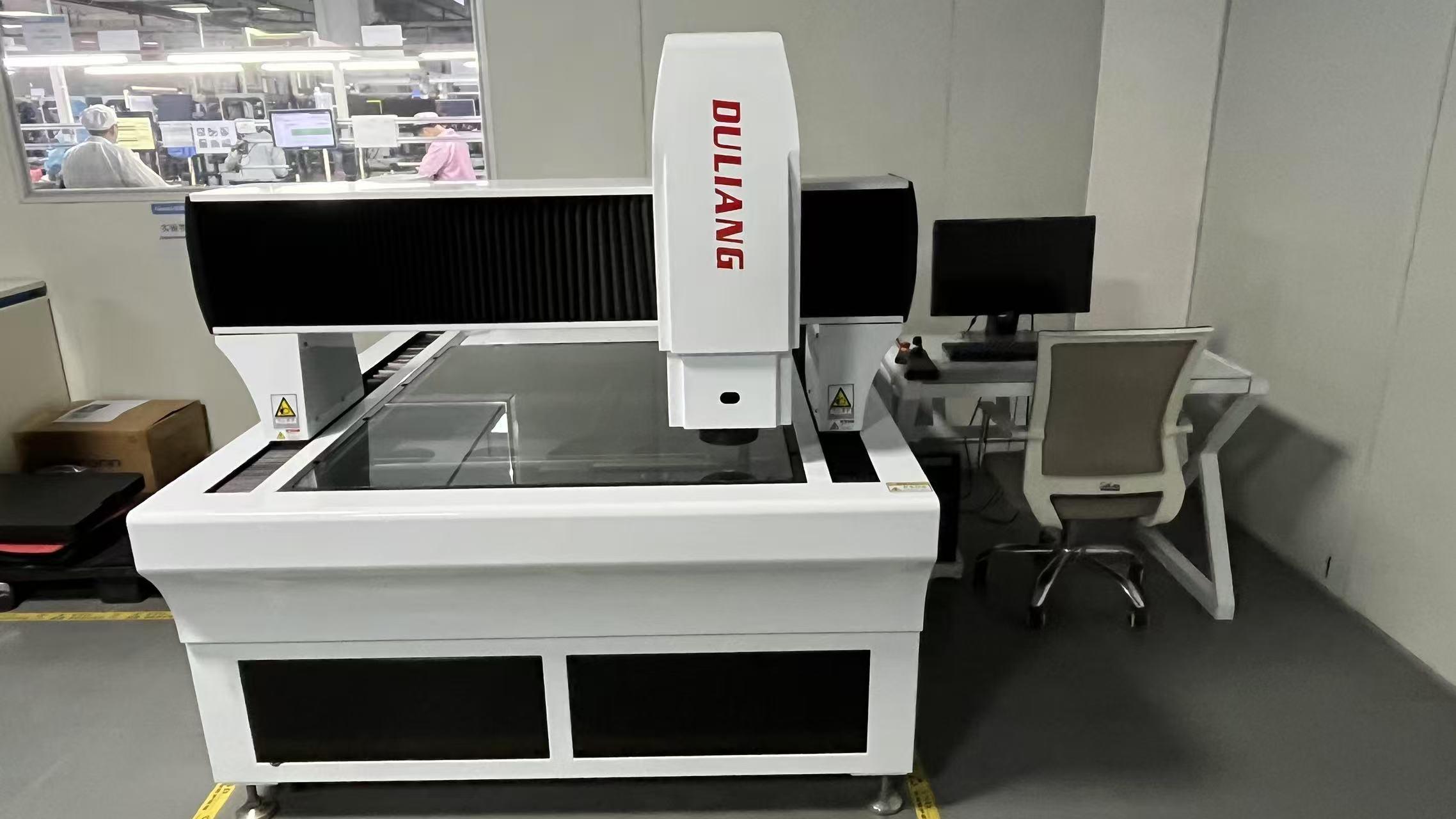
At CoreByte, quality assurance is an uncompromised standard. We utilize an ISO9001-based quality management structure, paired with Automated Optical Inspection (AOI), 3D X-ray microscopy, and intensive high-temperature burn-in/aging tests to eliminate infant mortality of electronic components. Our technical staff includes 45 dedicated quality control inspectors and 85 veteran R&D engineers, allowing us to roll out over 120 advanced product models annually.
How Chinese raw material access, advanced chemical etching capabilities, and logistics synergy benefit Luxembourg system integrators.
Procuring Thick Copper PCBs involves navigating challenges related to raw copper costs, chemical precision, and structural lamination integrity. Manufacturing thick copper boards in China leverages a highly consolidated electronics ecosystem, ensuring access to high-grade copper foils, customized high-TG laminates, and specialized chemical etching suppliers. CoreByte's integrated supply chain networks—partnering with over 1,200 raw material and component suppliers—provide uninterrupted manufacturing schedules even during global trade fluctuations.
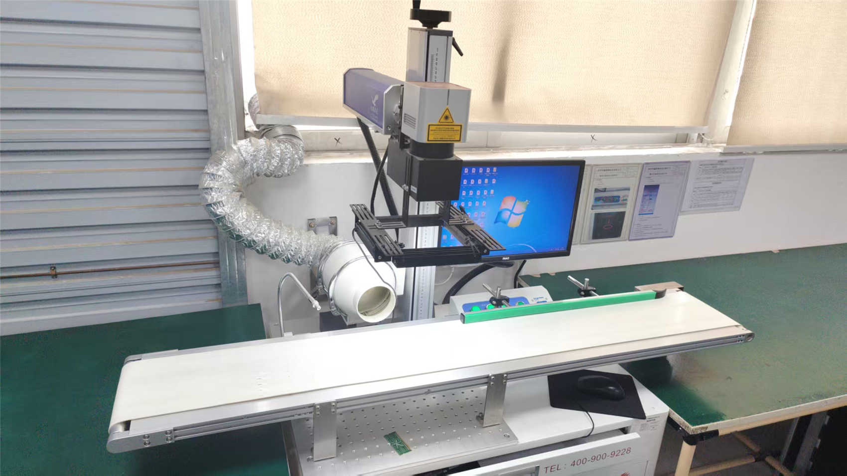
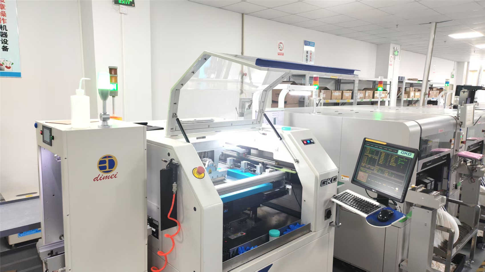
Through the implementation of Industry 4.0 smart factory practices, CoreByte utilizes robotic loading systems, direct-imaging lithography (LDI), and automated optical measurement tools to guarantee consistent trace profiles. This automation minimizes operator errors and significantly lowers production costs. For Luxembourgish engineering firms, this means a reliable transition from quick-turn prototype designs to high-volume assembly lines without quality degradation or extended lead times.
Luxembourg Findel Airport acts as one of the premier air cargo gateways in Europe. By organizing express air freight routes from China directly to Luxembourg, CoreByte guarantees seamless logistics and fast delivery times. Our customs and compliance team handles all importing steps, delivering critical industrial PCB assemblies directly to your production facility door in optimal timeframes.
Meeting rigorous European directives and providing engineering support from prototype to final deployment.
Entering the European and Luxembourgish markets requires strict compliance with environmental and electrical directives. CoreByte constructs every thick copper board to conform perfectly to active European Union standards. We ensure your products encounter zero compliance friction during end-system certification phases.
Select from our fully certified, high-frequency, thermal-performance product line, designed to run under strenuous electrical conditions.
Direct answers to the most common engineering and procurement questions raised by Luxembourgish system designers.
Partner with a premier thick copper PCB manufacturer to secure your high-power electronics supply chain. Get comprehensive engineering support, competitive pricing, and rapid delivery directly to your facility in Luxembourg.
* Our engineers will review your Gerber files and design requirements and respond within 24 business hours.