Direct-from-factory high-performance hardware systems, multilayer PCBs, and advanced cooling modules optimized for commercial, computational, and industrial infrastructures in North America.
The landscape of electronics manufacturing in the United States is undergoing a profound structural evolution. Driven by the demands of next-generation telecommunications, automated medical equipment, defense systems, and massive high-performance computing (HPC) clusters, the requirement for high-reliability multi-layer circuit boards has hit unprecedented heights. As American businesses shift their designs toward faster signal propagation and higher component density, traditional double-sided boards no longer suffice.
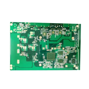
Modern US industries demand multi-layer PCBs (typically from 4 up to 32+ layers) that can manage complex routing topologies, implement rigid impedance matching, and survive challenging thermal environments. From aerospace hubs in Texas and California to telecom giants in the Pacific Northwest, engineering teams look to international manufacturers who can combine technological precision with scale.
Deploying heavy copper structures and high-temperature TG laminates designed to handle vibration, thermal cycles, and vacuum outgassing requirements typical of satellite systems and aviation control boards.
Supporting ultra-low-loss dielectric materials (e.g., Rogers, Panasonic Megtron 6/7) to ensure signal integrity across PCIe Gen 5/6 lanes and 112G PAM4 network architectures.
Providing high-density interconnect (HDI) boards that power compact MRI controllers, handheld diagnostic tools, and robotic surgical interfaces demanding absolute reliability.
For American OEM/ODM clients, choosing an international supplier is not merely about finding the lowest cost per square inch; it is a complex calculation of legal compliance, manufacturing standards, and supply chain continuity. An elite Multi-layer Circuit Board Exporter must possess deep familiarity with the regulatory structures that govern US imports and domestic electronics distribution.
Any PCB entering the United States must meet strict material safety guidelines. Our manufacturing processes fully support compliance with the RoHS (Restriction of Hazardous Substances) directive and REACH regulations, ensuring that lead, mercury, cadmium, and polybrominated biphenyls are minimized or eliminated entirely.
Additionally, for electronic applications targeting building interiors, consumer appliances, or industrial machinery, compliance with Underwriters Laboratories (UL) standards—specifically the UL 94V-0 flammability rating—is non-negotiable. Our boards carry permanent UL markings ensuring traceability and immediate passage through customs audits.
While IPC Class 2 governs general industrial electronics, aerospace, military, and life-support applications demand IPC-A-600 Class 3 compliance. This standard dictates near-zero tolerance for inner-layer misalignment, strict copper plating thicknesses in through-holes (minimum 1 mil), and zero voiding in lamination joints. Our quality control team executes cross-sectional analysis and micro-section reports for every batch destined for high-reliability US projects.
One of the primary friction points for US buyers is the time difference when dealing with offshore factories. To bridge this gap, we offer a dedicated North American customer care window coupled with 24/7 DFM (Design for Manufacturability) support.
The Pearl River Delta remains the undisputed global capital of electronics manufacturing. The velocity at which components can be sourced, substrates processed, and assemblies verified is unparalleled. For US organizations, partnering with a Chinese supplier that bridges the gap between memory systems design and advanced board fabrication yields massive strategic benefits.
Within a 50-mile radius of our facility lies a complete component-sourcing ecosystem. If a client design requires a rare passive component, high-performance thermal pad, or specialized chipset, we source it in hours rather than weeks. This proximity dramatically shortens the NPI (New Product Introduction) cycles, allowing US hardware startups to out-innovate competitors.
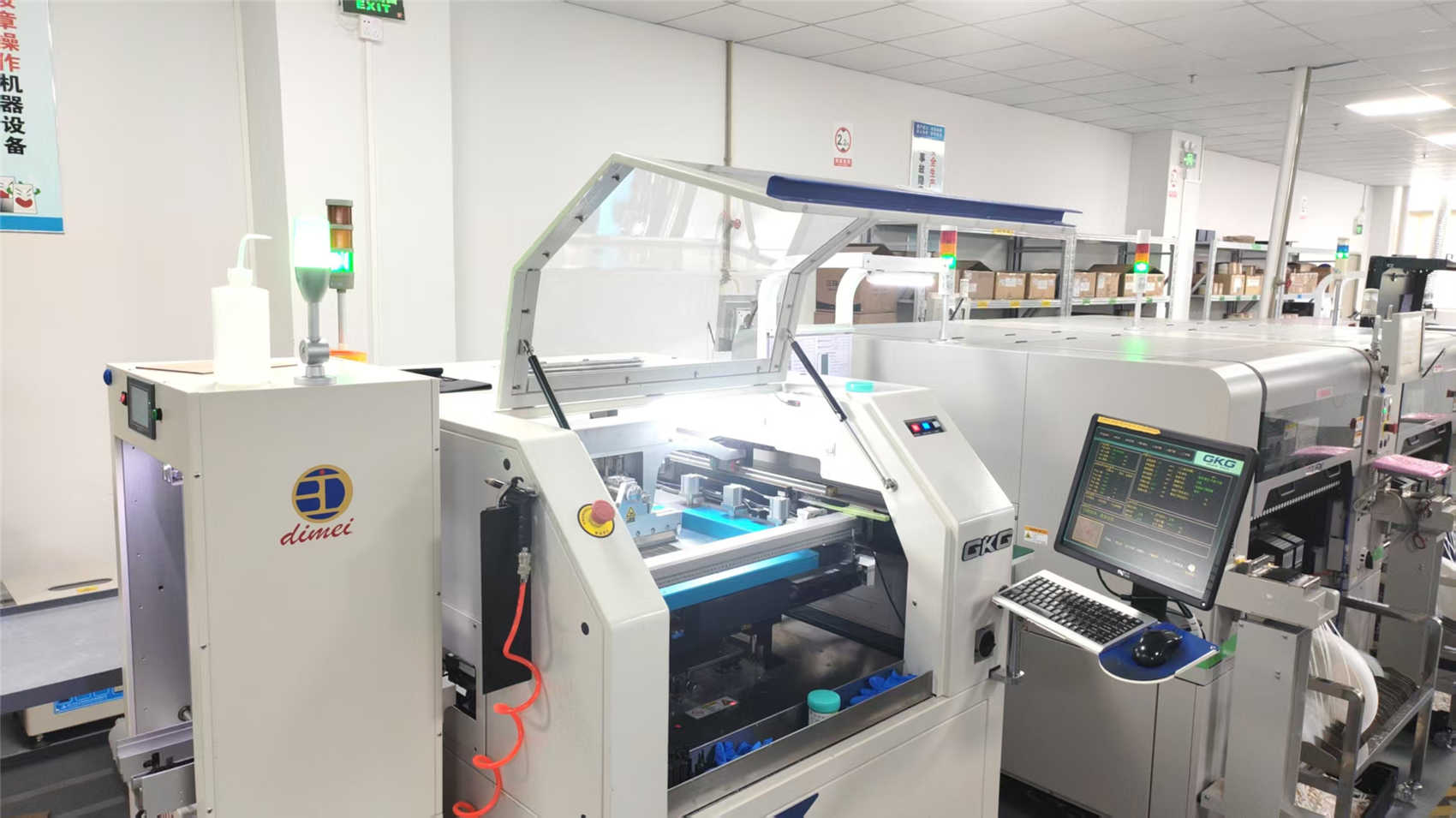
Established in 2016, CoreByte Storage Technology Co., Ltd. has positioned itself at the cutting edge of memory design and hardware integration. With an annual export footprint of USD 12 million, we rely on a strong quality management system based on ISO9001. We operate advanced Automated Optical Inspection (AOI) lines, 3D X-Ray Inspection (AXI) for BGA packages, and high-temperature aging chambers to guarantee performance.

The demand for increased circuit density and signal transmission speeds is accelerating several key technology trends in the multilayer circuit board industry:
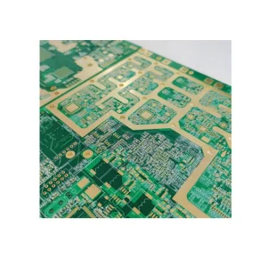
Integrating microvias, blind vias, and buried vias to stack layers in extremely small form factors, allowing shorter path routing for high-pin BGA chips.
Using advanced TDR (Time Domain Reflectometry) testing to ensure precise trace geometry and dielectric constant matching, avoiding high-frequency signal reflections.
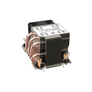
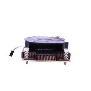
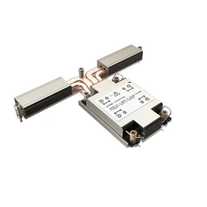
Embedding heavy copper cores, metal backings, or specialized thermal vias to manage waste heat generated by high-power server CPUs and high-current power stages.
Choosing the correct base laminate is the most critical decision in multilayer circuit design. The table below outlines the primary materials we process to meet varying performance tiers:
| Material Classification | Glass Transition Temp (Tg) | Dissipation Factor (Df) | Typical US Target Application |
|---|---|---|---|
| Standard FR-4 | 130°C - 140°C | ~0.020 | Consumer electronics, basic logic boards |
| High-TG FR-4 (Shengyi S1000-2) | 170°C - 180°C | ~0.015 | Industrial PCs, automotive, multi-layer server memory |
| Halogen-Free Laminates | 150°C - 170°C | ~0.012 | Green enterprise systems, eco-compliant products |
| Rogers RO4003C / RO4350B | >280°C | 0.0027 - 0.0037 | RF Microwave systems, radar, military communication |
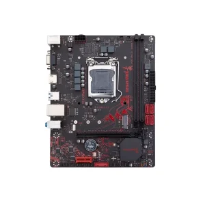
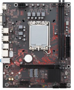
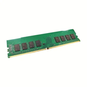
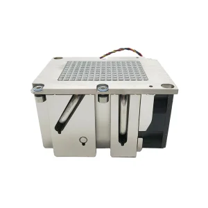
Explore our comprehensive range of high-density motherboard assemblies, low-latency RAM memory modules, and specialized thermal heat sinks built for 24/7 industrial and data center environments.
Executing a 12-layer or 24-layer stack-up configuration requires sophisticated manufacturing technology. At CoreByte, we utilize automated, state-of-the-art lamination presses that precisely control pressure, temperature, and cooling cycles. This prevents warpage and maintains mechanical stability.
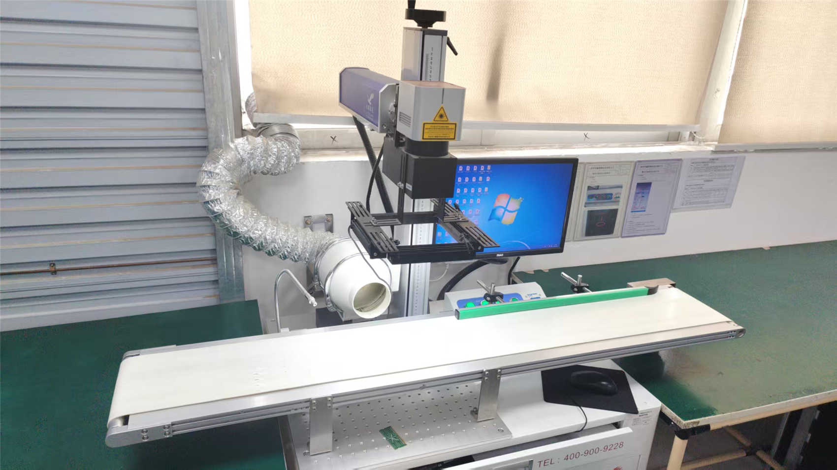
In high-frequency designs, even minor variations in dielectric thickness can disrupt trace impedance. We use high-precision laser direct imaging (LDI) systems to transfer circuit designs directly onto photo-sensitive dry films, eliminating the optical errors associated with traditional film contact exposures.
Additionally, our automated optical inspection (AOI) checks internal layers before lamination, catching potential shorts or opens early. For complex ball grid array (BGA) components, we use 3D X-ray systems to verify high-density assembly quality, ensuring reliable solder joints without micro-voids.
In-depth technical and logistical answers curated by our engineering division for procurement managers and hardware systems designers.
Connect with our engineering team today for a free design review, impedance analysis, and a detailed DFM assessment.