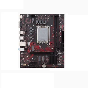
Berlin, recognized as one of Europe’s most dynamic hubs for Industry 4.0, IoT development, and automotive tech, requires a manufacturing partner that understands the intersection of speed and precision. While local manufacturing is essential, the scalability of Laser Stencils Manufacturers lies in the seamless integration between German design philosophy and high-efficiency production capacities in China.
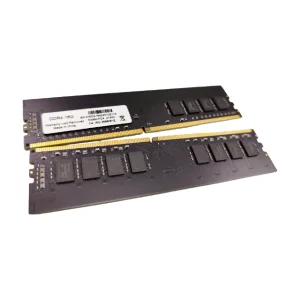
CoreByte Storage Technology Co., Ltd. serves as a critical bridge. By leveraging 9+ years of industry experience, we provide not just raw components, but complete assembly solutions for the Berlin tech market. Whether it is SMT (Surface Mount Technology) stencils for prototyping or large-scale PCB production, our commitment to ISO9001 standards ensures that Berlin engineers receive high-tolerance, reliable products every time.
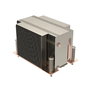
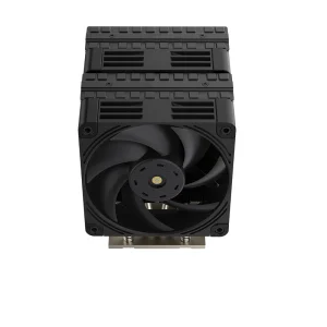
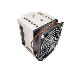
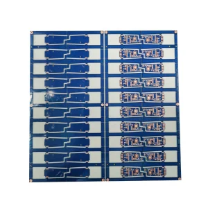
The manufacturing of laser stencils and PCBs has evolved beyond simple cutting processes. It is now about material science and heat dissipation.
In today's global landscape, supply chain resilience is paramount. CoreByte has established a robust ecosystem with over 1,200 supply chain partners. This ensures that even during global fluctuations, our delivery timelines to Berlin remain stable.
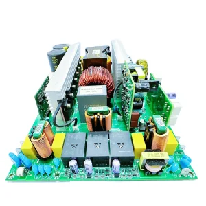
Our facility, spanning 320㎡ of high-tech production space, utilizes Automated Optical Inspection (AOI) and high-temperature aging tests. This is not just "manufacturing"; it is "quality assurance engineering." By outsourcing the labor-intensive stages of PCB assembly and stencil production to a specialized China factory, Berlin companies can focus their internal resources on R&D, software, and systems architecture.
Yes. Our team of 85 R&D engineers supports global clients with remote technical consultation, ensuring your Gerber files and stencil designs are optimized for production before the first cut is made.
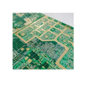
We strictly adhere to ISO9001 quality management systems. Our production processes for PCB assembly and laser cutting are fully compatible with RoHS and REACH regulations, critical for the European market.
With our established logistics network serving Southeast Asia, Europe, and North America, we utilize air and rail freight options to Berlin to balance cost and speed, ensuring timely arrival for just-in-time manufacturing schedules.
Absolutely. Customization is at the core of our business model. From frequency tuning to thermal solution adjustments and branding, we tailor our products to fit your specific market requirements.